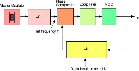
Pll stands for 'phase-locked loop' and is basically a closed loop frequency control system, which functioning is based on the phase sensitive detection of phase difference between the input and output signals of the controlled oscillator (co)
PLL stands for 'Phase-Locked Loop' and is basically a closed loop frequency control
system, which functioning is based on the phase sensitive detection of phase difference between
the input and output signals of the controlled oscillator (CO). Fig. 2 shows the classic
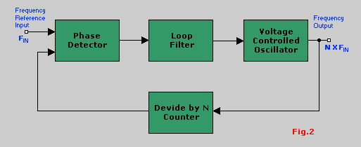
The phase detector is a device that compares two input frequencies, generating an output
that is a measure of their phase difference (if, for example, they differ in frequency, it gives a
periodic output at the difference frequency). If fIN doesn't equal fVCO, the phase-error signal, after
being filtered and amplified, causes the VCO frequency to deviate in the direction of fIN . If
conditions are right, the VCO will quickly "lock" to fIN maintaining a fixed relationship with the
At that point the filtered output of the phase detector is a dc signal, and the control input
to the VCO is a measure of the input frequency, with obvious applications to tone decoding
(used in digital transmission over telephone lines) and FM detection. The VCO output is a
locally generated frequency equal to fIN , thus providing a clean replica of fIN, which may itself
be noisy. Since the VCO output can be a triangle wave, sine wave, or whatever, this provides a
nice method of generating a sine wave, say, locked to a train of pulses. In one of the most
common applications of PLLs, a modulo-n counter is hooked between the VCO output and the
phase detector, thus generating a multiple of the input reference frequency fIN. This is an ideal
method for generating clocking pulses at a multiple of the power-line frequency for integrating
A/D converters (dual-slope, charge-balancing), in order to have infinite rejection of interference
at the power-line frequency and its harmonics. It also provides the basic technique of frequency
A basic Voltage Controlled Oscillator (VCO) can be seen in Fig. 3. It shows a basic
voltage controlled oscillator by which frequency of oscillation is determined by L1, C2, and D2.
D2 is a so-called varactor or varicap. Most common diodes will behave as a varicap when
reversed biased, but they must be operated below the junction breakdown parameters. With
reverse bias, this diode will act as a capacitor, its depletion zone forming the dielectric
properties. Changing the amount of reverse bias within the diode's breakdown limits, will alter
the depletion zone width and hence vary the effective capacitance presented by the diode. This in
turn changes the frequency resonancy of the oscillator circuit. But how does this help us? After
all, the VCO is not stable. Any slight voltage variation in the circuit will cause a shift in
frequency. If there was some way we could combine the flexibility of the VCO with the stability
of the crystal oscillator, we would have the ideal frequency synthesis system.
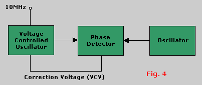
What if we feed the output of a VCO and Crystal Oscillator into a phase detector? What
is a Phase Detector? (See Fig. 4). It is similar to a discriminator or ratio detector used in
frequency demodulation or it could be a digital device, like an 'Exclusive OR' gate.
If two signals are fed into a phase detector, being equal in phase and frequency, there will be no
output from the detector. However, if these signals are not in phase and frequency, the difference
is converted to a DC output signal. The greater the frequency/phase difference in the two signals,
the larger the output voltage. Look at Fig. 4. The VCO and Crystal Oscillator outputs are
combined with a phase detector and any difference will result in a DC voltage output. Suppose
crystal oscillator frequency. This phenomena is referred to as Phase Locked Loop in its most
basic form. Only part of the VCO output needs to be sent to the phase detector. The rest can be
But hold on a minute, the VCO is locked onto the crystal oscillator and is therefore
behaving as if it were a fixed frequency oscillator. This gives us the stability of a crystal
oscillator, but lost the flexibility we were aiming for. We may just as well use the crystal
oscillator alone for all the good this arrangement has done to us. It certainly doesn't appear as if
Let's investigate how we can solve this problem. Suppose our crystal frequency was 10
MHz, but we wanted the VCO to operate on 20 MHz. The phase detector will of course detect a
frequency difference and pull the VCO down to 10 MHz, but what if we could fool the phase
detector into thinking the VCO was really only operating on 10 MHz, when in reality it is
operating on 20 MHz. Take a look at Fig. 5. Suppose, for example in Fig. 4 we used a divide-by-
four instead of the divide-by-two. Then, at LOCK, the VCO would be oscillating at 40 MHz yet
still be as stable as the crystal reference frequency.
There are oscillators that will operate over a large range of frequencies. Variable
Frequency Oscillators (VFO) are made to change frequency by changing the value of one of the
frequency determining circuits. A VCI is one in which this component is made to change
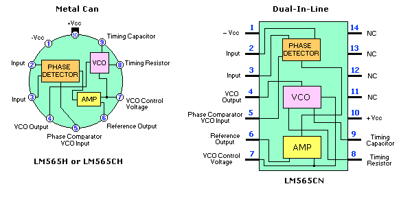
PLL Components Phase Detector: Let's have a look at the basic phase detector. There are actually two basic types,
sometimes referred to as Type I, and Type II. The Type I phase detector is designed to be driven
by analog signals or digital square-wave signals, whereas the Type II phase detector is driven by
digital transitions (edges). They are typified by the most common used 565 (linear Type I) and
the CMOS 4046, which contains both Type I and Type II. The simplest phase detector is the
Type I (digital), which is simply an Exclusive-OR gate
(see Fig. 5a.). With low-pass filtering, the graph of the
output voltage versus phase difference is as shown, for
input square-waves of 50% duty-cycle. The Type I
(linear) phase detector has similar output-voltage-versus-
phase characteristics, although its internal circuitry is actually a "four-quadrant multiplier", also
known as a "balanced mixer". Highly linear phase detectors of this type are essential for lock-in detection, which is a fine technique.
Todays engineers face constant challenges in the design of PLL circuits because of the
level of phase noise and the fundamental property of noise floor signals, especially in the design
of radio and wireless networks. More recently, switching speed of PLL's have become a critical
parameter in todays design of synthesizers, and especially for our modern networks such as 3G,
WLANs, WCDMA, and Bluetooth technology. The switching speed is emerging as a
challenging requirement for single loop, single chip PLL designs. Speed is mainly a function of
loop bandwidth, but in many cases the loop band width cannot be too wide because of phase
noise considerations. Speed-up techniques have been devised to improve PLL transient time, but
most of them have limited efficiency. In addition, speed-up techniques will have to be improved.
For the WCDMA and 3G markets (and others emerging) a reasonable goal is 100 to 150mS for a
dF=60Mhz excursion and a convergence to df=250Hz. One solution the industry will probably
adopt in the future is the use of highly complex Sigma Delta fractional PLL architectures, which
allow a high reference frequency and wide loop bandwidth, while maintaining resolution and a
good phase noise profile (low division). This technique is already being implemented today.
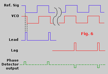
The type II phase detector is sensitive
only to the relative timing of edges
shown in Fig. 6.. The phase comparator
circuit generates either lead or lag output
output transitions occur before or after the
respectively. The width of these pulses is
equal to the time between the respective edges. The output circuitry then either sinks or sources
current (respectively) during those pulses and is otherwise open-circuited, generating an average
like that in Fig. 7. This is completely
input signals, unlike the situation with
earlier. Another nice feature of this phase
detector is the fact that the output pulses disappear entirely when the two signals are in lock. This
means that there is no "ripple" present at the output to generate periodic phase modulation in the
loop, as there is with the type I phase detector. Also, there is an additional difference between the
The type I detector is always generating an output wave, which must then be filtered by
the loop filter. Thus, in a PLL with type I phase detector, the loop filter acts as a low-pass filter,
smoothing this full-swing logic-output signal. There will always be residual ripple, and
consequent periodic phase variations, in such a loop. In circuits where phase-locked loops are
used for frequency multiplication or synthesis, this adds "phase-modulation sidebands" to the
By contrast, the type II phase detector generates output pulses only when there is a phase
error between the reference and the VCO signal. Since the phase detector output otherwise looks
like an open circuit, the loop filter capacitor then acts as a voltage-storage device, holding the
voltage that gives the right VCO frequency. If the reference signal moves away in frequency, the
phase detector generates a train of short pulses, charging (or discharging) the capacitor to the
new voltage needed to put the VCO back into lock.
The second-order PLL, serves as the basis for all PLL synthesizer designs and
technology. Most PLL designs, especially for synthesizers where third and fourth order loops are
common, use a different terminology, and deal mainly with the open loop gain and phase.
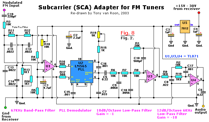
To see an example of a working PLL doing its job, check out the circuit below of Fig. 8.
This schematic diagram shows a so-called SCA adapter. The abbreviation "SCA" stands for
Subsidiary Communications Authorization. It is used for 'hidden' messages, music, etc. on a
normal hidden section of the FM band. It is based on a 67-KHz subcarrier that is placed on a
station's main FM carrier. It is even possible to have multiple subcarriers, some carrying digital
data, audio, data encryption, coded messages, and more. Subcarrier transmissions have no effect
on standard FM mono and stereo bands and are fully compatible with all existing radios. This
circuit can be hooked up to most fm tuners with a minimum of fuss. Low in cost, it uses just a
few readily available IC's. The use of a Printed Circuit Board for this design is recommended.
REGIONAL CANCER CENTRE MEDICAL COLLEGE CAMPUS TENDER NO.1/RCC/13:14 FOR ANTI CANCER DRUGS Competitive tenders in two bid system in separate sealed covers superscribed with the name and number of tender are invited from the Manufacturers/Direct Importers of Anti Cancer Drugs with Indian/ International market standing certificate of at least 3 years for the supply of Anti Cancer Drugs to Regio
— MESSAGE DISCLAIMER — These messages are offered for your personal edification and enrichment. There is no legal copyright on this material. I have used many sources, and I have always attempted to cite any exact quotations. Any failure to cite a quote is simply an oversight on my part. If you are a preacher or teacher, I encourage�
 PLL stands for 'Phase-Locked Loop' and is basically a closed loop frequency control
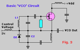
 A basic Voltage Controlled Oscillator (VCO) can be seen in Fig. 3. It shows a basic
 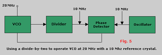 crystal oscillator frequency. This phenomena is referred to as Phase Locked Loop in its most
basic form. Only part of the VCO output needs to be sent to the phase detector. The rest can be
But hold on a minute, the VCO is locked onto the crystal oscillator and is therefore
behaving as if it were a fixed frequency oscillator. This gives us the stability of a crystal
oscillator, but lost the flexibility we were aiming for. We may just as well use the crystal
oscillator alone for all the good this arrangement has done to us. It certainly doesn't appear as if
Let's investigate how we can solve this problem. Suppose our crystal frequency was 10
MHz, but we wanted the VCO to operate on 20 MHz. The phase detector will of course detect a
frequency difference and pull the VCO down to 10 MHz, but what if we could fool the phase
detector into thinking the VCO was really only operating on 10 MHz, when in reality it is
operating on 20 MHz. Take a look at Fig. 5. Suppose, for example in Fig. 4 we used a divide-by-
crystal oscillator frequency. This phenomena is referred to as Phase Locked Loop in its most
basic form. Only part of the VCO output needs to be sent to the phase detector. The rest can be
But hold on a minute, the VCO is locked onto the crystal oscillator and is therefore
behaving as if it were a fixed frequency oscillator. This gives us the stability of a crystal
oscillator, but lost the flexibility we were aiming for. We may just as well use the crystal
oscillator alone for all the good this arrangement has done to us. It certainly doesn't appear as if
Let's investigate how we can solve this problem. Suppose our crystal frequency was 10
MHz, but we wanted the VCO to operate on 20 MHz. The phase detector will of course detect a
frequency difference and pull the VCO down to 10 MHz, but what if we could fool the phase
detector into thinking the VCO was really only operating on 10 MHz, when in reality it is
operating on 20 MHz. Take a look at Fig. 5. Suppose, for example in Fig. 4 we used a divide-by-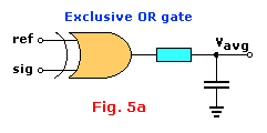
 Type I (digital), which is simply an Exclusive-OR gate
(see Fig. 5a.). With low-pass filtering, the graph of the
Type I (digital), which is simply an Exclusive-OR gate
(see Fig. 5a.). With low-pass filtering, the graph of the 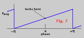 like that in Fig. 7. This is completely